Nokia | 8.1 Schematic Diagram
chipset integration, power management ICs (PMIC), and charging circuit paths. Technical Review of Repairability Reviewers and repair sites like
✅ Search for “Nokia 8.1 TA-1119 test point diagram” – often shared for unlocking or EDL mode. nokia 8.1 schematic diagram
: Technical repair guides often focus on "ways"—specific electrical paths for functions like LCD light , charging , and audio —to help identify broken traces or faulty components. Key Hardware Specifications System-on-Chip Qualcomm Snapdragon 710 (10 nm) Display 6.18-inch Full HD+ Charging USB Type-C (sub-board integrated) Storage/RAM 64GB/4GB or 128GB/6GB options Sensors Fingerprint (rear-mounted), Proximity, Accelerometer Resources for Repair & Schematics Nokia 8.1 in 2023 review scorched component near the
A full schematic diagram typically includes the motherboard layout, component IDs, and electrical pathing (ways). You can find these documents on technical repositories and through specialized repair tools: power management ICs (PMIC)
: A reliable repository for service manuals. You can find the Nokia 8.1 User and Service Manual
He traced a line back to a tiny, scorched component near the
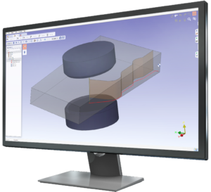
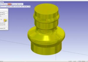
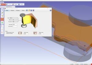
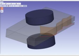
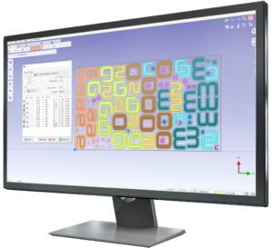
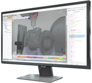
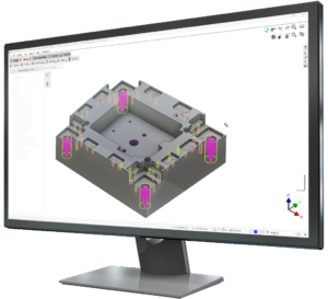
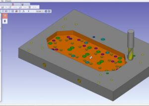
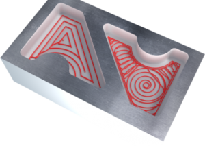
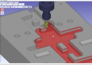
 Sviluppata da GO2cam International, millyuGO® è la risposta alle problematiche specifiche delle produzioni che necessitano di un’asportazione di materiale considerevole.
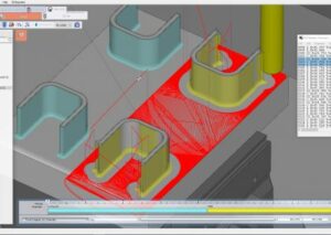
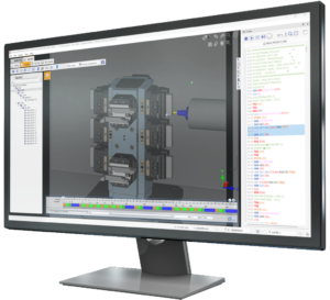
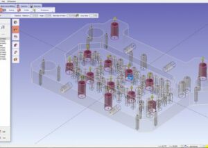
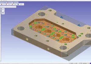
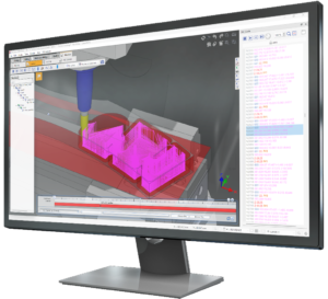